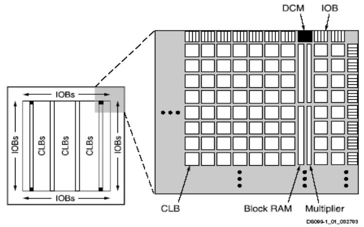
FPGA:Field Programmable Gate Arrays
Composed of:
- CLBs (Configurable Logic Blocks): Perform logic 可编程逻辑功能块
- IOBs (input/output Buffers): interface with outside world I/O
- Programmable interconnection: connect CLBs and IOBs 片内互连线
- other: multipliers and RAMs
CLBs (Configurable Logic Blocks)
Composed of:
- LUTs (LookUp Tables): perform combinational logic 查找表
- Flip-flops (FF): perform sequential functions 触发器
- Multiplexers: connect LUTs and flip-flops 多路复用器

- logic elements LE 可编程逻辑单元介绍:
- 只用LUT实现组合逻辑
- 只用D触发器就是打一拍
- LUT和DFF都用即实现复杂时序逻辑
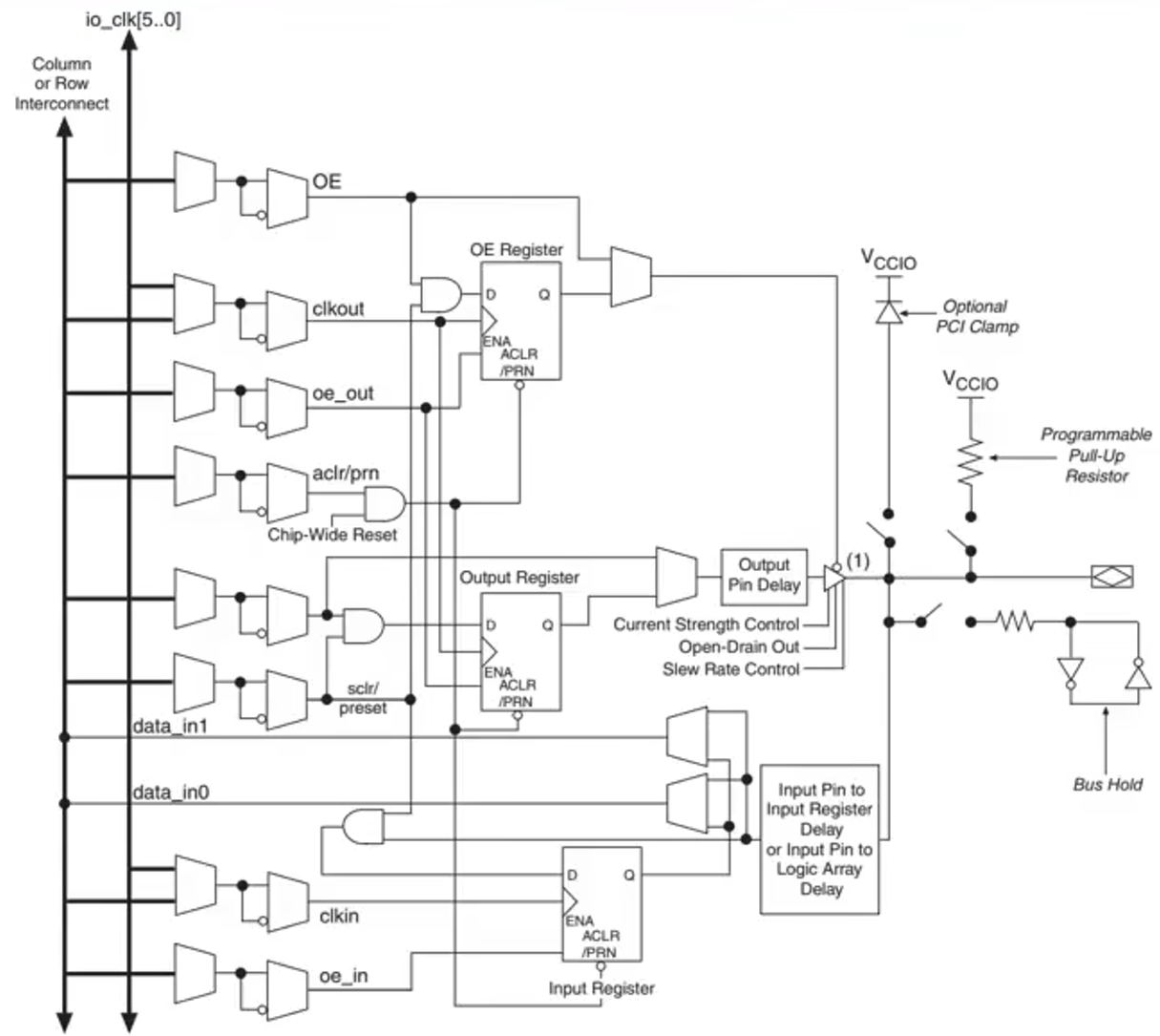
I/O(input/output Buffers)
- 输出寄存器 output register
- 输入寄存器 input register
- 输出使能寄存器(控制输入输出开关)OE register
- 输出延迟链 output pin delay
- 输入延迟链 input pin delay
- 上拉电阻 IIC
Programmable interconnection 可编程内部互联资源
- 各种长度的连线线段
- 可编程连接开关
FPGA Design Flow
- A CAD tool (such as Vivado)is used to design and implement a digital system.
- The user enters the design using schematic entry or an HDL.
- Correct functionality is verified using simulation
- A synthesis tool maps your description onto the FPGA.
- The result is a bitfile that contains configures the CLBs and the connections between them and the lOBs.
- The bitfile is downloaded to the FPGA